- 您现在的位置:买卖IC网 > Sheet目录312 > AT25128AW-10SU-2.7 (Atmel)IC EEPROM 128KBIT 20MHZ 8SOIC
�� �
�
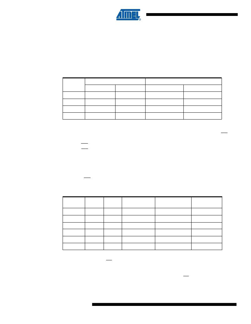
�WRITE� STATUS� REGISTER� (WRSR):� The� WRSR� instruction� allows� the� user� to� select� one� of�
�four� levels� of� protection.� The� AT25128A/256A� is� divided� into� four� array� segments.� Top� quarter�
�(1/4),� top� half� (1/2),� or� all� of� the� memory� segments� can� be� protected.� Any� of� the� data� within� any�
�selected� segment� will� therefore� be� read� only.� The� block� write� protection� levels� and� correspond-�
�ing� status� register� control� bits� are� shown� in� Table� 3-4� .�
�The� three� bits,� BP0,� BP1,� and� WPEN� are� nonvolatile� cells� that� have� the� same� properties� and�
�functions� as� the� regular� memory� cells� (e.g.� WREN,� t� WC� ,� RDSR).�
�Table� 3-4.�
�Block� Write� Protect� Bits�
�Status� Register� Bits�
�Array� Addresses� Protected�
�Level�
�0�
�1(1/4)�
�2(1/2)�
�3(All)�
�BP1�
�0�
�0�
�1�
�1�
�BP0�
�0�
�1�
�0�
�1�
�AT25128A�
�None�
�3000� –� 3FFF�
�2000� –� 3FFF�
�0000� –� 3FFF�
�AT25256A�
�None�
�6000� –� 7FFF�
�4000� –� 7FFF�
�0000� –� 7FFF�
�The� WRSR� instruction� also� allows� the� user� to� enable� or� disable� the� write� protect� (WP)� pin�
�through� the� use� of� the� write� protect� enable� (WPEN)� bit.� Hardware� write� protection� is� enabled�
�when� the� WP� pin� is� low� and� the� WPEN� bit� is� “1”.� Hardware� write� protection� is� disabled� when�
�either� the� WP� pin� is� high� or� the� WPEN� bit� is� “0”.� When� the� device� is� hardware� write� protected,�
�writes� to� the� Status� Register,� including� the� Block� Protect� bits� and� the� WPEN� bit,� and� the� block-�
�protected� sections� in� the� memory� array� are� disabled.� Writes� are� only� allowed� to� sections� of� the�
�memory� which� are� not� block-protected.�
�NOTE:� When� the� WPEN� bit� is� hardware� write� protected,� it� cannot� be� changed� back� to� “0”,� as�
�long� as� the� WP� pin� is� held� low.�
�Table� 3-5.�
�WPEN� Operation�
�Protected�
�Unprotected�
�Status�
�WPEN�
�0�
�0�
�1�
�1�
�X�
�X�
�WP�
�X�
�X�
�Low�
�Low�
�High�
�High�
�WEN�
�0�
�1�
�0�
�1�
�0�
�1�
�Blocks�
�Protected�
�Protected�
�Protected�
�Protected�
�Protected�
�Protected�
�Blocks�
�Protected�
�Writable�
�Protected�
�Writable�
�Protected�
�Writable�
�Register�
�Protected�
�Writable�
�Protected�
�Protected�
�Protected�
�Writable�
�READ� SEQUENCE� (READ):� Reading� the� AT25128A/256A� via� the� SO� pin� requires� the� follow-�
�ing� sequence.� After� the� CS� line� is� pulled� low� to� select� a� device,� the� Read� op-code� is� transmitted�
�via� the� SI� line� followed� by� the� byte� address� to� be� read� (see� Table� 3-6� on� page� 11� ).� Upon� com-�
�pletion,� any� data� on� the� SI� line� will� be� ignored.� The� data� (D7� -� D0)� at� the� specified� address� is�
�then� shifted� out� onto� the� SO� line.� If� only� one� byte� is� to� be� read,� the� CS� line� should� be� driven� high�
�after� the� data� comes� out.� The� read� sequence� can� be� continued� since� the� byte� address� is� auto-�
�matically� incremented� and� data� will� continue� to� be� shifted� out.� When� the� highest� address� is�
�10�
�AT25128A_256A�
�3368J–SEEPR–06/07�
�发布紧急采购,3分钟左右您将得到回复。
相关PDF资料
AT25160B-XHL-T
IC EEPROM 16KBIT 20MHZ 8TSSOP
AT25256B-SSHL-B
IC EEPROM 256KBIT 20MHZ 8SOIC
AT25256T2-10TI-2.7
IC EEPROM 256KBIT 3MHZ 20TSSOP
AT25320AY6-10YH-1.8
IC EEPROM 32KBIT 20MHZ 8DFN
AT25640T1-10TI-2.7
IC EEPROM 64KBIT 3MHZ 14TSSOP
AT25DF321-SU
IC FLASH 32MBIT 70MHZ 8SOIC
AT25F1024AN-10SU-2.7
IC FLASH 1MBIT 33MHZ 8SOIC
AT25F2048N-10SU-2.7
IC FLASH 2MBIT 33MHZ 8SOIC
相关代理商/技术参数
AT25128A-W2.7-11
制造商:ATMEL 制造商全称:ATMEL Corporation 功能描述:SPI Serial EEPROMs
AT25128AY4-10YU-1.8
制造商:ATMEL 制造商全称:ATMEL Corporation 功能描述:SPI Serial EEPROMs
AT25128B
制造商:ATMEL 制造商全称:ATMEL Corporation 功能描述:serial electrically-erasable programmable read only memory
AT25128B-CUL-T
制造商:Atmel Corporation 功能描述:
AT25128B-MAHL-T
功能描述:电可擦除可编程只读存储器 128K Density SPI 16,384 x 8 Organ RoHS:否 制造商:Atmel 存储容量:2 Kbit 组织:256 B x 8 数据保留:100 yr 最大时钟频率:1000 KHz 最大工作电流:6 uA 工作电源电压:1.7 V to 5.5 V 最大工作温度:+ 85 C 安装风格:SMD/SMT 封装 / 箱体:SOIC-8
AT25128B-SSHL-B
功能描述:电可擦除可编程只读存储器 128K Density SPI 16,384 x 8 Organ RoHS:否 制造商:Atmel 存储容量:2 Kbit 组织:256 B x 8 数据保留:100 yr 最大时钟频率:1000 KHz 最大工作电流:6 uA 工作电源电压:1.7 V to 5.5 V 最大工作温度:+ 85 C 安装风格:SMD/SMT 封装 / 箱体:SOIC-8
AT25128B-SSHL-T
功能描述:电可擦除可编程只读存储器 128K Density SPI 16,384 x 8 Organ RoHS:否 制造商:Atmel 存储容量:2 Kbit 组织:256 B x 8 数据保留:100 yr 最大时钟频率:1000 KHz 最大工作电流:6 uA 工作电源电压:1.7 V to 5.5 V 最大工作温度:+ 85 C 安装风格:SMD/SMT 封装 / 箱体:SOIC-8
AT25128B-SSHL-T
制造商:Atmel Corporation 功能描述:Serial EEPROM IC